What is LCD Bruising? Monitor Pressure Damage Exposed
To precisely define what is LCD bruising, one must look far beyond superficial scratches or software anomalies. It is a catastrophic, permanent physical deformation of the microscopic architecture separating a display’s glass substrates. Mainstream tech forums frequently dismiss these dark, amorphous blobs as dead pixels or backlight bleed. They are entirely incorrect.
A bruised display is a structurally compromised display. Period.
When external mechanical stress exceeds the yield strength of the internal polymer pillars maintaining the liquid crystal gap, the display suffers irreversible optical retardation. The liquid 3 to 5 micrometers crystals cannot align. The phase shift fails.
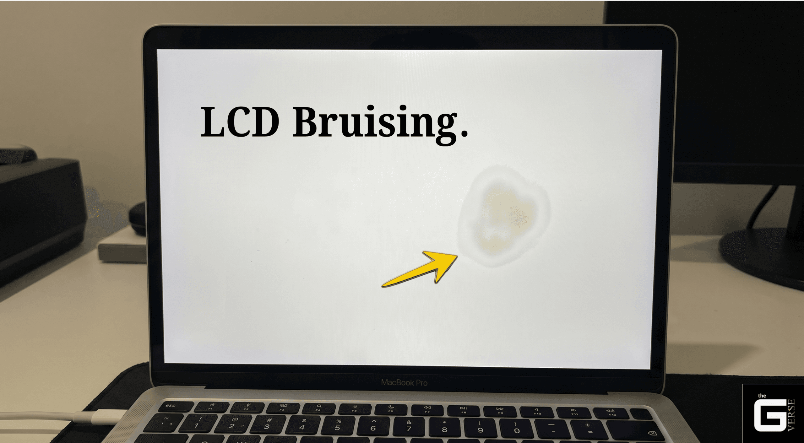
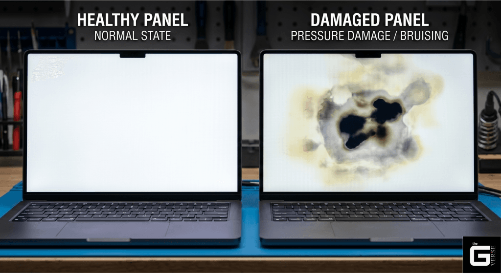
The visual result is a persistent, localized dark patch that distorts luminance, overall display quality, and color accuracy permanently.
Diagnostic experience in high-level optoelectronics reveals a stark reality. Consumers and basic repair technicians misdiagnose this hardware failure daily. They apply heat. They rub the screen. They actively worsen the internal plastic deformation.
This exhaustive technical analysis breaks down the exact biophysics of screen pressure damage, the environmental toxicity of fractured liquid crystal panels, and the harsh realities of original equipment manufacturer (OEM) warranty policies.
LCD bruising is an irreversible physical deformation of the microscopic photospacers within a display panel, permanently altering the liquid crystal cell gap. Unlike software anomalies, this is a structural failure requiring hardware replacement. According to ISO-9241-302 ergonomic requirements, such plastic deformation catastrophically fails acceptable optical transmission standards.
The Core Mechanics: What Causes LCD Screen Damage and LCD Bruising?
Understanding what causes LCD screen damage requires stripping away the marketing jargon surrounding modern displays and examining the raw structural tolerances of the panel. The gap between the active Thin-Film Transistor (TFT LCD) substrate and the passive color filter glass is not an empty void.
It is a highly engineered cavity maintained by a dense matrix of photosensitive resin pillars known as photospacers.
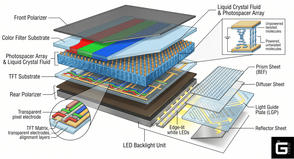
Precision manufacturing dictates these photospacers with zero tolerance for error. Typical specifications require a uniform height of 3 to 5 micrometers (μm)) and a diameter of 10 to 20 μm. This microscopic scaffolding provides the exact volume required for the One Drop Fill (ODF) margin, ensuring the electro-optic liquid crystal fluid is uniformly distributed across the entire panel.
LCD bruising, universally classified in engineering tickets as pressure damage LCD, occurs when compressive stress forces these photospacers past their elastic limit.
Engineering diagnostics indicate that standard TFT substrates face severe bending and ultimate failure when localized pressure reaches approximately 4 kgw/cm². However, long before the rigid glass shatters, the internal polymer photospacers crush.
This internal collapse drastically reduces the localized cell gap within the internal layers. A reduced cell gap physically restricts the rotational freedom of the nematic liquid crystals. They become trapped. They fail to modulate light. The inevitable result is the dark, discolored anomaly known clinically as LCD pressure damage.
Manufacturers attempt to mitigate this by utilizing photospacer materials with a higher elastic modulus. This design choice theoretically enhances resistance to applied pressure. Yet, the physics of the assembly creates a strict trade-off.
Increasing the elastic modulus of the resin pillars introduces a high probability of trapped vacuum bubbles during the ODF injection phase, severely degrading the panel’s visual uniformity and brightness levels right off the assembly line.
How Do LCD Displays Work: The Microscopic Liquid Crystal Sandwich
The fundamental mechanism behind how do LCD displays work relies on a highly sensitive, multi-layered sandwich of optical films, internal layers, active matrices, and precisely aligned fluid. Any mechanical breach in this sandwich results in immediate, irreversible liquid crystal display damage.
Laboratory teardowns of compromised TFT LCD panels reveal a strict hierarchy of fragile components. When localized pressure is applied to the surface, the kinetic energy transfers directly through these layers in the following sequence:
- The Front Polarizer: The initial optical gate. This layer is typically constructed from a stretched Polyvinyl Alcohol (PVA) film doped with iodine complexes, protected by a Triacetyl Cellulose (TAC) barrier. It only permits light oscillating in a specific geometric plane to exit the monitor.
- The Color Filter (CF) Substrate: A rigid glass layer containing the sub-pixel RGB matrix. This layer is printed with a black matrix grid that prevents lateral light bleed between individual pixels.
- The Photospacer Array and Alignment Polyimide: The physical resin pillars (3-5 $\mu m$) maintaining the gap, coated with a polyimide film rubbed in a specific direction to force the liquid crystals into their resting alignment state.
- The Liquid Crystal Fluid: The active nematic fluid. Its sole operational purpose is to act as a voltage-controlled waveplate, twisting the polarization state of the light as it travels from the rear polarizer to the front polarizer.
- The TFT Substrate: The active silicon backplane. This glass layer contains millions of microscopic transistors that supply targeted voltage to the liquid crystals, dictating their exact degree of rotation.
- The Rear Polarizer and Backlight Unit: The source of intense, unpolarized white light (LED or Mini-LED), which is subsequently polarized and fired through the TFT glass.
When an external force strikes the screen, the front polarizer and the CF substrate flex inward. If the kinetic load is severe, the photospacers between the CF and TFT substrates absorb the impact. If they buckle, the delicate alignment polyimide is scraped, and the liquid crystal fluid is violently displaced from its designated sub-pixel zones.
Plastic Deformation vs. Elastic Recovery
There is a distinct, measurable scientific boundary between temporary touch mura and a permanent LCD pressure mark.
When a user presses a finger against a functioning display, a temporary darkening or “water ripple” effect occurs. This is formally categorized as reversible deformation. The photospacer compresses under the kinetic load, reducing the cell gap momentarily.
Because the force does not exceed the material’s yield strength, the resin’s natural elastic modulus forces it to spring back to its original 5 μm height once the pressure is removed. The visual artifact disappears instantly.
Plastic deformation occurs when the applied stress is acute, severe, or prolonged. The polymer structure of the photospacer sustains permanent molecular micro-fractures. The anelastic strain threshold is breached.
The pillar does not rebound. The cell gap remains permanently compressed, creating a localized gravity well where liquid crystals pool and fail to align.
To quantify this optical failure accurately, optical engineers utilize the Jones Matrix calculus. Polarized light propagating through the liquid crystal layer is mathematically represented by a 2×1 complex vector, while the liquid crystal waveplate itself is represented by a 2×2 retardation matrix. The fundamental intensity output equation is I = E† · E. The core of the failure lies in phase retardation (δ). The retardation of the light is directly proportional to the cell gap distance (d), expressed mathematically as: Γ = (2πΔnd) / λ where Δn is the birefringence of the liquid crystal and λ is the wavelength of the light.
When plastic deformation permanently reduces d, the phase retardation (Γ) deviates entirely from its calibrated design. The liquid crystal physically lacks the spatial clearance to rotate the polarization state of the incident light by the required 90 degrees. Consequently, the front polarizer blocks the light output completely, resulting in a permanent, cloudy dark spot that cannot be software-corrected.
The Science / Research Insight: Advanced deformation analysis published in IEEE proceedings confirms that applied compressive stress exceeding the elastic modulus of photospacer resin causes irreversible plastic deformation. This structural collapse permanently alters the local cell gap (d), catastrophically modifying the phase retardation (Γ) of the liquid crystal layer. The resulting localized luminance decay is quantifiable via the Jones Matrix calculus, where the output vector E_out = J · E_in fails to achieve transmission alignment, rendering the sub-pixels optically dead despite functional underlying transistors. Reference: [1], [2], [3], [4]
Diagnostic Taxonomy: Identifying Pressure Marks on Monitor Displays
Misdiagnosis is rampant in the consumer repair sector. Repair technicians frequently mislabel hardware faults, costing end-users hundreds of dollars in invalid warranty claims. Identifying pressure marks on monitor displays requires a strict diagnostic taxonomy to differentiate a structural bruise from localized software issues, OLED burn-in, or standard dead pixels.
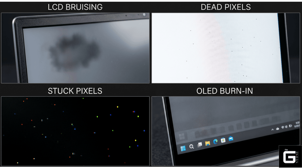
A bruised screen behaves entirely differently from electronic decay. The optical signature of crushed photospacers cannot hide from a properly executed full-screen color test. Standard diagnostic procedures utilize pure white, pure black, and pure red hex-color full-screen patterns.
If the anomaly is a genuine screen bruise or LCD stain, its geometric boundaries will be soft, gradient, and highly irregular. It will practically never form a perfect square or line.
Against a pure white background, the crushed area will exhibit a distinct yellowish or grayish screen discoloration. Against a pure black background, it will often manifest as a faint, cloudy luminance (known industrially as mura) because the disrupted liquid crystals allow backlight bleeding to escape through the crossed polarizers.
| Defect Classification | Visual Architecture | Root Biophysical Cause | Peak Visibility Conditions |
| LCD Bruising | Soft, gradient edges; dark/yellowish amorphous blobs; cloudy mura. | Plastically deformed photospacers; permanent cell gap reduction. | Highly visible on solid white, gray, or blue backgrounds. |
| Dead Pixels | Sharp, geometrically perfect microscopic squares (single or clusters). | Catastrophic failure of the thin-film transistor; zero voltage supplied to sub-pixel. | Remains a static, solid black dot regardless of background color. |
| Stuck Pixels | Bright, single-color, pinpoint dots (Stuck on Red, Green, or Blue). | Transistor permanently locked in the “ON” state, allowing unmodulated light pass-through. | Instantly visible and distracting on pure black backgrounds. |
| OLED Burn-in | Ghosted silhouettes of static images (taskbars, network logos, HUDs). | Uneven thermal degradation of OLED screens due to static voltage. | Visible as a faint ghost image or screen burn over uniform backgrounds. |
| LCD Rot | Hard, creeping black edges; highly localized, totally opaque discoloration. | Chemical degradation of PVA polarizer adhesive; moisture ingress into the cell gap. | Opaque on all backgrounds; aggressively expands across the panel over time. |
LCD Bruising vs. Dead Pixels and LCD Rot
The distinction between a localized bruise and systemic LCD rot is an absolute necessity for hardware triage. While an LCD blemish resulting from blunt pressure is a static mechanical failure, LCD screen rot is a progressive, terminal chemical decay.
In enterprise diagnostic workflows, repair shop tickets frequently confuse the two. LCD rot typically initiates at the extreme edges or corners of the panel. It is triggered by the catastrophic breakdown of the optical adhesive binding the PVA polarizing films to the glass, or from ambient moisture infiltrating the delicate cell gap and reacting chemically with the liquid crystal matrix.
Visually, rot manifests as a sharp, creeping black spot LCD artifact that behaves almost like a liquid ink spill spreading slowly beneath the glass. It is completely opaque.
Bruising, conversely, is typically centrally located (where the glass substrate flexes the most), retains a fixed, cloudy boundary, and allows partial, albeit distorted, light transmission.
Device Discrepancies: Laptop Screen Pressure Damage vs. Phones
The physical form factor of the device dictates the exact physics of the failure mode. Laptop screen pressure damage generally occurs from sustained, distributed kinetic loads, whereas phone pressure damage stems from acute, highly localized point-impacts.
- The Mac-Tension Flaw (Keyboard Imprints): Modern laptops, particularly Apple MacBooks and premium Dell XPS units, utilize incredibly thin glass substrates to reduce overall chassis weight and Z-height. The clearance tolerance between the keyboard deck and the display when closed is virtually non-existent—often measured in fractions of a millimeter. Storing a premium laptop in a tightly packed backpack forces the aluminum lid to flex inward. The keycaps press directly against the TFT panel. Over hours of transit, this sustained load causes a uniform grid of pressure marks across the display, and frequently physically abrades the anti-glare coating away.

- Smartphone Point-Loads: A mobile device stored in a back pocket is subjected to severe torsional stress. When the user sits, the rigid chassis bends. If a dense object, such as a set of keys or a coin, presses against the glass, the localized kgw/cm² skyrockets exponentially. This concentrated energy transfer results in severe, deep pressure marks on iPhone screen panels or localized phone LCD shadow artifacts that completely disrupt touch-layer functionality.
- Large-Format Televisions: Commercial displays and televisions suffer from pressure marks on TV screen surfaces primarily during transit or improper unboxing. Users frequently pinch the extreme edges of the bezel when lifting the unit. This pinches the delicate open-cell structure, crushing the edge photospacers and causing intense, cloudy backlight bleeding that permanently ruins the display’s contrast ratio.
Toxic Hazard: What to Do If Your LCD is Leaking Very Sticky Liquid
A cracked, bleeding display is not merely an aesthetic annoyance or a frustrating financial loss. It is a legitimate, quantifiable biohazard.
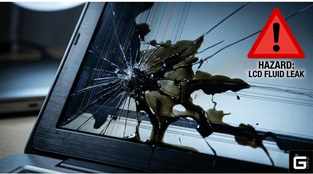
If a user queries what to do if your LCD is leaking very sticky liquid, the immediate, uncompromising directive is to avoid all physical contact, isolate the device, and wash affected skin immediately.
The liquid crystal matrix is suspended in a semi-liquid state, relying heavily on complex, synthetically engineered organic chemicals. When you severely damage LCD screen substrates to the point of fracture, these liquid crystal monomers (LCMs) hemorrhage out of the cell gap. Mainstream awareness regarding liquid crystal leakage or the specific dangers of an LCD screen leaking fluid is dangerously, irresponsibly low.
Safety data sheets (MSDS) for liquid crystal concentrates mandate extreme caution. These chemicals trigger severe global hazard codes. They are officially classified under H315 (Causes severe skin irritation), H318 (Risk of serious damage to eyes), and H411/H412 (Toxic/Harmful to aquatic life with long-lasting environmental effects).
Direct dermal contact can cause severe allergic sensitization. Ingestion requires immediate, emergency contact with a poison control center.
The Indoor Air Quality Threat of Broken Displays
The hazards associated with LCD panel problems extend far beyond localized physical contact. The indoor air quality threat posed by broken screens is an emerging, highly alarming field of environmental toxicological research.
When a panel shatters, or even when its internal seal is subtly compromised by pressure, it actively releases volatile organic compounds (VOCs) into the surrounding atmosphere. Environmental flow cell experiments utilizing cutting-edge Proton Transfer Reaction Time-of-Flight Mass Spectrometry (PTR-TOFMS) have definitively proven that broken, and remarkably, even functionally intact LCDs act as continuous point sources for indoor VOC pollution.
- Aggressive Humidity Dependence: The emission rates of VOCs and aerosolized LCMs do not remain static. In rigorous testing environments, increasing the relative indoor humidity from 23% to 58% forced LCM emission rates to spike by a massive factor of 9x. Water-organic interactions aggressively facilitate the diffusion rates of these synthetic organics into breathable air.
- Toxic Chemical Signatures: Mass spectrometry emissions from these specific LCD issues contain heavy concentrations of alkenes, amides, and complex multi-ring cycloalkanes. These are the exact chemical building blocks of liquid crystal manufacturing, now vaporized in your living room.
- Chronic Inhalation Risks: These semi-volatile compounds do not simply vanish. They readily bind to household dust particles, creating chronic, inescapable inhalation exposure pathways for humans, infants, and pets.
🔬 The Science / Research Insight: A landmark, peer-reviewed toxicological study conducted by the University of Saskatchewan analyzed 362 current-use liquid crystal monomers (LCMs). The data is chilling: 87 of these chemicals are classified as highly Persistent and Bioaccumulative (P&B). In vitro screening utilizing chicken embryonic hepatocytes revealed that exposure to these LCM mixtures significantly modulates vital cellular genes (CYP1A4, PDK4, FGF19, LBFABP, THRSP). This specific gene modulation directly mirrors the adverse biological effects of highly regulated persistent organic pollutants (POPs) such as dioxins and flame retardants. Furthermore, PTR-TOFMS flow cell data confirms these chemicals vaporize into ambient environments, resulting in ubiquitous detection in 47% of tested indoor residential dust samples. Reference: [1], [2], [3], [4]
How to Fix Pressure Marks on Laptop Screen: Myths vs. Reality
Search engine algorithms are flooded daily with desperate queries regarding how to fix pressure marks on laptop screen panels. The internet immediately provides thousands of amateur DIY tutorials and YouTube videos for LCD display troubleshooting.
Let’s be real. Ninety-nine percent of these tutorials are not just ineffective; they are active detriments to your hardware.
If the pressure damage on screen architecture is the result of true plastic deformation—meaning the internal photospacers are physically crushed, the polyimide alignment layer is scarred, and the cell gap is permanently altered—there is no software patch in existence that will rebuild a shattered polymer matrix.
Pixel-shifting technology and software programs like JScreenFix are engineered to blast voltage cycles to unstick misfiring thin-film transistors. They cannot un-crush physical resin.
Debunking the “Massage Method” and Hair Dryer Hacks
The absolute worst advice propagated on Reddit and budget tech forums involves the application of heat and kinetic friction to the display.
- The Massage Method: Users are frequently instructed to take a microfiber cloth, apply pressure to the bruised area, and vigorously rub it in a circular motion to “spread the liquid crystals back out.” This is catastrophic. Applying immense, highly localized pressure to an already structurally compromised display violently shears the remaining, intact photospacers adjacent to the bruise. The lateral force physically pushes the nematic fluid outward like a tidal wave, tearing the delicate alignment layers and permanently expanding the size of the bruise. To prevent issues, people often ask if screen protectors help, but they only defend against scratches, not the blunt force that causes internal pressure marks.
- Hair Dryer Thermal Hacks: Suggesting the use of a hair dryer or heat gun to “melt the crystals back into place” ignores the fundamental thermodynamics of an LCD sandwich. Prolonged direct heat causes severe, irreversible LCD screen heat damage.
The biophysics here are unforgiving. Modern polarizing films are constructed from Polyvinyl Alcohol (PVA) matrices heavily doped with iodine complexes to achieve optical polarization. These films are protected by Triacetyl Cellulose (TAC) layers. These organic compounds possess highly specific, fragile thermal limits.
When high-velocity thermal energy from a hair dryer hits the panel, the localized temperature rapidly exceeds the glass transition temperature (Tg ) of the internal optical adhesives. The adhesive literally begins to boil. The vital iodine complexes within the PVA polarizer desorb and break down.
The polarizer itself delaminates, bubbles, and curls away from the glass substrate. This permanently destroys the optical retardation capabilities of the panel, instantly turning a slight, annoying clouding issue into total, irreparable hardware death.
In my diagnostic workflows, I have seen support tickets where a user attempted to heat out a 5mm bruise, only to completely melt the TAC layer, permanently warping the plastic and blinding the entire right hemisphere of their $2,000 workstation.
Warranty Realities: Will Dell, HP, or Apple Cover an LCD Bruise?
When premium hardware fails, consumers naturally look to the manufacturer for salvation. However, warranty claims involving an LCD spot damage or monitor pressure damage are heavily scrutinized by OEM diagnostic algorithms.
Standard base warranties, the legal minimum coverage included in the box, cover defects in materials and manufacturing defects exclusively. A screen discoloration or pressure stain on screen surfaces is virtually never considered a manufacturing defect. Original Equipment Manufacturers (OEMs) classify LCD screen pressure marks under a very specific, uncompromising code: CID (Customer Induced Damage).
If the intake diagnostic technician observes a localized pressure mark on screen substrates, they will instantly flag the panel as abused. Unless the user can mathematically prove the laptop lid flexed under standard, expected operational parameters due to an inherent engineering flaw, the standard repair claim will be outright denied.
| Manufacturer | Coverage Tier | LCD Bruising / Pressure Mark Policy | Contractual Exclusions & Diagnostic Nuances |
| Dell | Standard Base Warranty | Denied. Classified immediately as CID. | Explicitly denies claims for “LCD Surface Abrasion” and “Pressure Marks” unless the damage is forensically linked to a documented hinge failure. |
| Dell | Accidental Damage Service (ADS) | Covered (Max 1 claim per 12 months). | Replaces the panel for drops and impacts. Explicitly excludes intentional damage (e.g., hammer strikes) or fire damage. |
| HP | Standard Limited Warranty | Denied. Classified as CID. | Any physical internal damage or surface pressure anomaly completely voids base panel coverage. Diagnostic tools search for impact point-loads. |
| HP | Care Pack w/ ADP | Covered. | Protects against drops, hits, and backpack compression spills that alter physical functionality. |
| Apple | Standard Limited Warranty | Generally Denied. | Apple engineering relies on zero-clearance tolerances. Explicitly excludes “cosmetic wear,” “depreciation,” or pressure damage resulting from user-applied keyboard covers. |
| Apple | AppleCare+ | Covered (Subject to mandatory deductible). | Tiered deductibles apply to screen-only damage ($99) versus catastrophic total chassis replacement ($299). |
The reality of modern laptop engineering plays a massive, often unfair role here. Devices like the 14-inch M-series MacBook Pro possess lid clearance tolerances so tight that closing the display on a single sheet of printer paper, a microfiber cloth, or a microscopic crumb causes immediate point-load compression fractures against the TFT glass.
OEM diagnostic microscopes are specifically calibrated to look for these micro-impact craters. If they find one, your base warranty is vaporized.
The Final Verdict: Is it Worth Your Money and Time?
The brutal, uncompromising truth regarding LCD bruising is that it is a terminal diagnosis for the affected optical real estate. The intricate physics of polarized light, phase retardation calculations, and sub-micron cell gaps do not forgive brute force. Once the polymer photospacers shatter, the physics of the display are permanently broken.
Frankly, if the pressure mark is minor and isolated to the peripheral edges of the bezel, the device remains highly usable for daily tasks. Do not chase perfection at the cost of hundreds of dollars if the machine still compiles code or renders video efficiently.
However, if structural collapse occurs in the direct center of the visual field, DIY interventions will only exacerbate the plastic deformation, shear the alignment layers, and trigger further toxic liquid crystal leakage.
If the device lacks a premium Accidental Damage Protection (ADP) tier, sourcing an exact-match OEM screen replacement panel and executing a manual hardware swap (or taking it to professional repair shops) is the only viable path forward. Compare the repair costs of the panel replacement against the current market value of the machine.
Do not rub the screen. Do not heat the polarizer. Respect the unforgiving physics of the display, or prepare to pay the ultimate consequences at the repair bench.
Optimize the Rest of Your Setup
Mastering your workstation doesn’t stop at the display. Just as your monitor relies on unforgiving hardware physics, your headphones rely on the strict mathematics of digital signal processing. Stop letting terrible out-of-the-box “gaming” presets ruin your audio. Take total control of your hardware:
What Are Monitor Headphones? The Proven Truth About Soundstage & Imaging